下面的链接提供了较新版本的源码
ver4.0源码下载:
ver3.1源码下载:
ver3.0源码下载:
ver2.2源码下载:
ver2.1源码下载:
ver2.1源码下载:
ver2.0源码下载:


version2.0是根据我上一个版本的uboot修改而来的,可以下载源码 后参照下面的内容进行修改 。
ver2.1源码下载:
ver1.0源码下载:
网络部分修改过程:
1. 在include/configs/tiny210.h 添加下述宏
红字部分与dm9000 相关的关键内容. 下面对关键部分作简要分析:
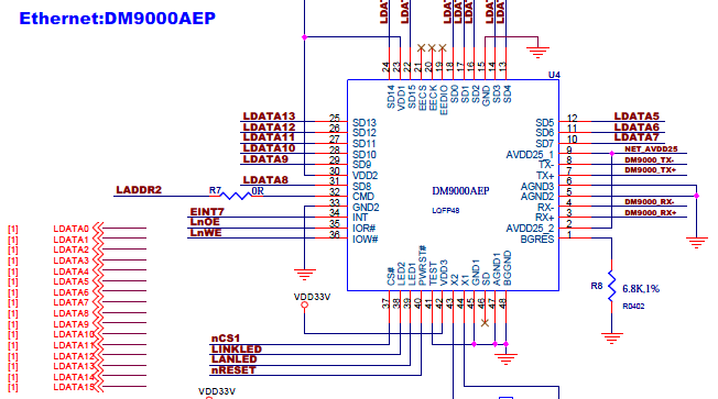
另外根据友善提供的linux-2.6.35 内核,参考其中dm9000的初始化配置,
#define S5PV210_PA_DM9000_A (0x88001000)
#define S5PV210_PA_DM9000_F (S5PV210_PA_DM9000_A + 0x300C)static struct resource dm9000_resources[] = {
[0] = { .start = S5PV210_PA_DM9000_A, .end = S5PV210_PA_DM9000_A + SZ_1K*4 - 1, .flags = IORESOURCE_MEM, }, [1] = { .start = S5PV210_PA_DM9000_F, .end = S5PV210_PA_DM9000_F + SZ_1K*4 - 1, .flags = IORESOURCE_MEM, }, [2] = { .start = IRQ_EINT(7), .end = IRQ_EINT(7), .flags = IORESOURCE_IRQ | IORESOURCE_IRQ_HIGHLEVEL, },};
可以分别得到
2.修改common/cmd_date.c

前两次修改的u-boot写SD卡的过程存在问题,虽然保存环境变量到SD能够成功,但是会有Writing to MMC(0)... mmc_send_cmd: error during transfer: 0x00208001 mmc write failed,这样的提示。而且每次启动只能够保存一次环境变量,若再次写SD卡会有failed提示并无法保存。这一次更新修复了这两个bug。
ver2.1源码下载:
下面的链接提供了前两次修改的源码
ver1.0源码下载:
ver2.0源码下载:你还可以参考下面两篇blog从头构建自己的u-boot for tiny210
ver2.1的基本功能:
1. SD boot,基于linaro u-boot的SPL功能实现
2. 从SD卡的FAT分区上加载文件到SDRAM
3. 将环境变量保存至SD卡
4. 添加DM9000网卡驱动,开启网络功能(例如:tftp,nfs等)
5. 添加TAB键命令自动补全功能
+6.修复bug:
修复bug 1:SD卡保存环境变量出现Writing to MMC(0)... mmc_send_cmd: error during transfer: 0x00208001 mmc write failed。
修复bug 2:每次启动只能保存一次环境变量。
ver2.1代码改动量非常小,一步就可完成,但是由于经验不足,我在bug的定位上花了很多时间.
具体修改如下:
测试saveenv:

PS : 简单记录解决过程
错误的打印出处的确不难找,printf("%s: error during transfer: 0x%08x\n", __func__, mask);即是.可是仔细看看被屏蔽部分代码是没什么问题的,
if (mask & (1 << 15)) {

前三个版本都不支持nandflash的读写,这次更新(ver2.2)添加了nandflash驱动及yaffs文件系统的烧写功能。在kasim的建议下我从ver2.2开始用git源代码仓库管理我的源码。并发布上一版本的补丁文件。
你可以点击下面的链接浏览u-boot for tiny210 ver2.2 源码:下面的提供了在CSDN资源库的下载链接:
ver2.2源码下载:
下面的提供了补丁包的下载链接:
ver2.2补丁下载:
下面的链接提供了前几次修改的源码:
ver1.0源码下载:
ver2.0源码下载:ver2.1源码下载:你还可以参考下三篇blog从头构建自己的u-boot for tiny210
ver2.2的基本功能:
1. SD boot,基于linaro u-boot的SPL功能实现
2. 从SD卡的FAT分区上加载文件到SDRAM
3. 将环境变量保存至SD卡
4. 添加DM9000网卡驱动,开启网络功能(例如:tftp,nfs等)
5. 添加TAB键命令自动补全功能
6.修复bug:
修复bug 1:SD卡保存环境变量出现Writing to MMC(0)... mmc_send_cmd: error during transfer: 0x00208001 mmc write failed。
修复bug 2:每次启动只能保存一次环境变量。
+7.添加NandFlash驱动,开启所有Nand cmd。
+8.添加Yaffs文件系统烧写支持。
参照本文后面内容修改完后:
启动:
部分NAND CMD测试:
下面简要介绍ver2.2的修改步骤:
左边的数字为旧行号,右边的数字为新行号,大家可以对应行号阅读修改部分的源码,或自己从ver2.1修改至ver2.2
1. 在此目录下修改Makefile
| 31 | 31 | ||
| 32 | 32 | ifdef CONFIG_SPL_BUILD | |
| 33 | 33 | COBJS += mmc_boot.o | |
| 34 | #COBJS += nand.o | ||
| 35 | #COBJS += nand_cp.o | ||
| 34 | 36 | endif | |
| 37 | COBJS += nand.o | ||
| 38 | COBJS += nand_cp.o | ||
| 35 | 39 | ||
| 36 | 40 | SOBJS := lowlevel_init.o mem_setup.o | |
| 37 | 41 |
| 17 | int add_mtd_device(struct mtd_info *mtd) |
| 64 | 64 | * Add MTD device so that we can reference it later | |
| 65 | 65 | * via the mtdcore infrastructure (e.g. ubi). | |
| 66 | 66 | */ | |
| 67 | sprintf(dev_name[i], "nand%d", i); | ||
| 67 | #if CONFIG_NAND_NO_USE_CHIP_NAME | ||
| 68 | sprintf(dev_name[i], "nand%d", i); | ||
| 68 | 69 | mtd->name = dev_name[i++]; | |
| 70 | #endif | ||
| 69 | 71 | add_mtd_device(mtd); | |
| 72 | |||
| 70 | 73 | #endif | |
| 71 | 74 | } else | |
| 72 | 75 | mtd->name = NULL; |
| 430 | 430 | #define CONFIG_CMDLINE_EDITING | |
| 431 | 431 | #define CONFIG_AUTO_COMPLETE | |
| 432 | 432 | #define CONFIG_SYS_HUSH_PARSER | |
| 433 | |||
| 434 | /*****************************Modified by lk for nand driver*************/ | ||
| 435 | #define CONFIG_CMD_NAND | ||
| 436 | #if defined(CONFIG_CMD_NAND) | ||
| 437 | #define CONFIG_CMD_NAND_YAFFS | ||
| 438 | #define CONFIG_CMD_MTDPARTS | ||
| 439 | #define CONFIG_SYS_MAX_NAND_DEVICE 1 | ||
| 440 | #define CONFIG_SYS_NAND_BASE (0xB0E000000) | ||
| 441 | #define NAND_MAX_CHIPS 1 | ||
| 442 | |||
| 443 | #define CONFIG_MTD_DEVICE /* needed for mtdparts commands add by lkmcu */ | ||
| 444 | |||
| 445 | #define NAND_DISABLE_CE() (NFCONT_REG |= (1 << 1)) | ||
| 446 | #define NAND_ENABLE_CE() (NFCONT_REG &= ~(1 << 1)) | ||
| 447 | #define NF_TRANSRnB() do { while(!(NFSTAT_REG & (1 << 0))); } while(0) | ||
| 448 | #define CONFIG_CMD_NAND_YAFFS_SKIPFB | ||
| 449 | |||
| 450 | #define CONFIG_NAND_USE_CHIP_NAME 1 | ||
| 451 | |||
| 452 | #if 0 | ||
| 453 | |||
| 454 | #define CONFIG_MTD_DEBUG | ||
| 455 | #define CONFIG_MTD_DEBUG_VERBOSE | ||
| 456 | |||
| 457 | #define CFG_NAND_SKIP_BAD_DOT_I 1 | ||
| 458 | #define CFG_NAND_HWECC | ||
| 459 | |||
| 460 | #define CONFIG_NAND_BL1_8BIT_ECC | ||
| 461 | #endif | ||
| 462 | #undef CFG_NAND_FLASH_BBT | ||
| 463 | #endif | ||
| 464 | |||
| 465 | |||
| 433 | 466 | #endif /* __CONFIG_H */ |
| 126 | 126 | uint32_t eccpos[128]; | |
| 127 | 127 | uint32_t oobavail; | |
| 128 | 128 | struct nand_oobfree oobfree[MTD_MAX_OOBFREE_ENTRIES]; | |
| 129 | uint32_t useecc; | ||
| 130 | uint32_t reserved; | ||
| 129 | 131 | }; | |
| 130 | 132 | ||
| 131 | 133 | /** |
- #include <common.h>
- #if defined(CONFIG_CMD_NAND)
- #include <nand.h>
- #include <bedbug/regs.h>
- #include <s5pc110.h>
- #include <asm/io.h>
- #include <asm/errno.h>
- /* Nand flash definition values by jsgood */
- #define S3C_NAND_TYPE_UNKNOWN 0x0
- #define S3C_NAND_TYPE_SLC 0x1
- #define S3C_NAND_TYPE_MLC 0x2
- #undef S3C_NAND_DEBUG
- /* Nand flash global values by jsgood */
- int cur_ecc_mode = 0;
- int nand_type = S3C_NAND_TYPE_UNKNOWN;
- /* Nand flash oob definition for SLC 512b page size by jsgood */
- static struct nand_ecclayout s3c_nand_oob_16 = {
- .useecc = MTD_NANDECC_AUTOPLACE, /* Only for U-Boot */
- .eccbytes = 4,
- .eccpos = {1, 2, 3, 4},
- .oobfree = {
- {.offset = 6,
- . length = 10}}
- };
- /* Nand flash oob definition for SLC 2k page size by jsgood */
- static struct nand_ecclayout s3c_nand_oob_64 = {
- .useecc = MTD_NANDECC_AUTOPLACE, /* Only for U-Boot */
- .eccbytes = 16,
- .eccpos = {40, 41, 42, 43, 44, 45, 46, 47,
- 48, 49, 50, 51, 52, 53, 54, 55},
- .oobfree = {
- {.offset = 2,
- .length = 38}}
- };
- /* Nand flash oob definition for MLC 2k page size by jsgood */
- static struct nand_ecclayout s3c_nand_oob_mlc_64 = {
- .useecc = MTD_NANDECC_AUTOPLACE, /* Only for U-Boot */
- .eccbytes = 32,
- .eccpos = {
- 32, 33, 34, 35, 36, 37, 38, 39,
- 40, 41, 42, 43, 44, 45, 46, 47,
- 48, 49, 50, 51, 52, 53, 54, 55,
- 56, 57, 58, 59, 60, 61, 62, 63},
- .oobfree = {
- {.offset = 2,
- .length = 28}}
- };
- /* Nand flash oob definition for 4Kb page size with 8_bit ECC */
- static struct nand_ecclayout s3c_nand_oob_128 = {
- .useecc = MTD_NANDECC_AUTOPLACE,
- .eccbytes = 104,
- .eccpos = {
- 24, 25, 26, 27, 28, 29, 30, 31,
- 32, 33, 34, 35, 36, 37, 38, 39,
- 40, 41, 42, 43, 44, 45, 46, 47,
- 48, 49, 50, 51, 52, 53, 54, 55,
- 56, 57, 58, 59, 60, 61, 62, 63,
- 64, 65, 66, 67, 68, 69, 70, 71,
- 72, 73, 74, 75, 76, 77, 78, 79,
- 80, 81, 82, 83, 84, 85, 86, 87,
- 88, 89, 90, 91, 92, 93, 94, 95,
- 96, 97, 98, 99, 100, 101, 102, 103,
- 104, 105, 106, 107, 108, 109, 110, 111,
- 112, 113, 114, 115, 116, 117, 118, 119,
- 120, 121, 122, 123, 124, 125, 126, 127},
- .oobfree = {
- {.offset = 2,
- .length = 22}}
- };
- #if defined(S3C_NAND_DEBUG)
- /*
- * Function to print out oob buffer for debugging
- * Written by jsgood
- */
- static void print_oob(const char *header, struct mtd_info *mtd)
- {
- int i;
- struct nand_chip *chip = mtd->priv;
- printk("%s:\t", header);
- for(i = 0; i < 64; i++)
- printk("%02x ", chip->oob_poi[i]);
- printk("\n");
- }
- #endif
- /*
- * Hardware specific access to control-lines function
- * Written by jsgood
- */
- static void s3c_nand_hwcontrol(struct mtd_info *mtd, int dat, unsigned int ctrl)
- {
- unsigned int cur;
- #if 1
- if (ctrl & NAND_CTRL_CHANGE) {
- if (ctrl & NAND_NCE) {
- if (dat != NAND_CMD_NONE) {
- cur = readl(NFCONT);
- /* Forced Enable CS */
- cur &= ~NFCONT_CS;
- writel(cur, NFCONT);
- }
- } else {
- cur = readl(NFCONT);
- /* Forced Enable CS */
- cur |= NFCONT_CS;
- writel(cur, NFCONT);
- }
- }
- if (dat != NAND_CMD_NONE) {
- if (ctrl & NAND_CLE)
- writeb(dat, NFCMMD);
- else if (ctrl & NAND_ALE)
- writeb(dat, NFADDR);
- }
- #endif
- }
- /*
- * Function for checking device ready pin
- * Written by jsgood
- */
- static int s3c_nand_device_ready(struct mtd_info *mtdinfo)
- {
- while (!(readl(NFSTAT) & NFSTAT_RnB)) {}
- return 1;
- }
- /*
- * We don't use bad block table
- */
- static int s3c_nand_scan_bbt(struct mtd_info *mtdinfo)
- {
- return nand_default_bbt(mtdinfo);
- }
- #if defined(CFG_NAND_HWECC)
- /*
- * Function for checking ECCEncDone in NFSTAT
- * Written by jsgood
- */
- static void s3c_nand_wait_enc(void)
- {
- while (!(readl(NFECCSTAT) & NFSTAT_ECCENCDONE)) {}
- }
- /*
- * Function for checking ECCDecDone in NFSTAT
- * Written by jsgood
- */
- static void s3c_nand_wait_dec(void)
- {
- while (!(readl(NFECCSTAT) & NFSTAT_ECCDECDONE)) {}
- }
- /*
- * Function for checking ECC Busy
- * Written by jsgood
- */
- static void s3c_nand_wait_ecc_busy(void)
- {
- while (readl(NFECCSTAT) & NFESTAT0_ECCBUSY) {}
- }
- /*
- * This function is called before encoding ecc codes to ready ecc engine.
- * Written by jsgood
- */
- static void s3c_nand_enable_hwecc(struct mtd_info *mtd, int mode)
- {
- u_long nfcont, nfconf;
- cur_ecc_mode = mode;
- nfconf = readl(NFCONF);
- if (nand_type == S3C_NAND_TYPE_SLC)
- nfconf &= ~NFCONF_ECC_MLC; /* SLC */
- else
- nfconf |= NFCONF_ECC_MLC; /* MLC */
- writel(nfconf, NFCONF);
- printf("NFCONF = %x\n",nfconf);
- /* Initialize & unlock */
- nfcont = readl(NFCONT);
- nfcont |= NFCONT_INITMECC;
- nfcont &= ~NFCONT_MECCLOCK;
- if (nand_type == S3C_NAND_TYPE_MLC) {
- if (mode == NAND_ECC_WRITE)
- nfcont |= NFCONT_ECC_ENC;
- else if (mode == NAND_ECC_READ)
- nfcont &= ~NFCONT_ECC_ENC;
- }
- writel(nfcont, NFCONT);
- }
- /*
- * This function is called immediately after encoding ecc codes.
- * This function returns encoded ecc codes.
- * Written by jsgood
- */
- static int s3c_nand_calculate_ecc(struct mtd_info *mtd, const u_char *dat, u_char *ecc_code)
- {
- u_long nfcont, nfmecc0, nfmecc1;
- /* Lock */
- nfcont = readl(NFCONT);
- nfcont |= NFCONT_MECCLOCK;
- writel(nfcont, NFCONT);
- if (nand_type == S3C_NAND_TYPE_SLC) {
- nfmecc0 = readl(NFMECC0);
- ecc_code[0] = nfmecc0 & 0xff;
- ecc_code[1] = (nfmecc0 >> 8) & 0xff;
- ecc_code[2] = (nfmecc0 >> 16) & 0xff;
- ecc_code[3] = (nfmecc0 >> 24) & 0xff;
- } else {
- if (cur_ecc_mode == NAND_ECC_READ)
- s3c_nand_wait_dec();
- else {
- s3c_nand_wait_enc();
- nfmecc0 = readl(NFMECC0);
- nfmecc1 = readl(NFMECC1);
- ecc_code[0] = nfmecc0 & 0xff;
- ecc_code[1] = (nfmecc0 >> 8) & 0xff;
- ecc_code[2] = (nfmecc0 >> 16) & 0xff;
- ecc_code[3] = (nfmecc0 >> 24) & 0xff;
- ecc_code[4] = nfmecc1 & 0xff;
- ecc_code[5] = (nfmecc1 >> 8) & 0xff;
- ecc_code[6] = (nfmecc1 >> 16) & 0xff;
- ecc_code[7] = (nfmecc1 >> 24) & 0xff;
- }
- }
- return 0;
- }
- /*
- * This function determines whether read data is good or not.
- * If SLC, must write ecc codes to controller before reading status bit.
- * If MLC, status bit is already set, so only reading is needed.
- * If status bit is good, return 0.
- * If correctable errors occured, do that.
- * If uncorrectable errors occured, return -1.
- * Written by jsgood
- */
- static int s3c_nand_correct_data(struct mtd_info *mtd, u_char *dat, u_char *read_ecc, u_char *calc_ecc)
- {
- int ret = -1;
- u_long nfestat0, nfestat1, nfmeccdata0, nfmeccdata1, nfmlcbitpt;
- u_char err_type;
- if (nand_type == S3C_NAND_TYPE_SLC) {
- /* SLC: Write ecc to compare */
- nfmeccdata0 = (read_ecc[1] << 16) | read_ecc[0];
- nfmeccdata1 = (read_ecc[3] << 16) | read_ecc[2];
- writel(nfmeccdata0, NFMECCDATA0);
- writel(nfmeccdata1, NFMECCDATA1);
- /* Read ecc status */
- nfestat0 = readl(NFESTAT0);
- err_type = nfestat0 & 0x3;
- switch (err_type) {
- case 0: /* No error */
- ret = 0;
- break;
- case 1: /* 1 bit error (Correctable)
- (nfestat0 >> 7) & 0x7ff :error byte number
- (nfestat0 >> 4) & 0x7 :error bit number */
- printk("s3c-nand: 1 bit error detected at byte %ld, correcting from "
- "0x%02x ", (nfestat0 >> 7) & 0x7ff, dat[(nfestat0 >> 7) & 0x7ff]);
- dat[(nfestat0 >> 7) & 0x7ff] ^= (1 << ((nfestat0 >> 4) & 0x7));
- printk("to 0x%02x...OK\n", dat[(nfestat0 >> 7) & 0x7ff]);
- ret = 1;
- break;
- case 2: /* Multiple error */
- case 3: /* ECC area error */
- printk("s3c-nand: ECC uncorrectable error detected\n");
- ret = -1;
- break;
- }
- } else {
- /* MLC: */
- s3c_nand_wait_ecc_busy();
- nfestat0 = readl(NFESTAT0);
- nfestat1 = readl(NFESTAT1);
- nfmlcbitpt = readl(NFMLCBITPT);
- err_type = (nfestat0 >> 26) & 0x7;
- /* No error, If free page (all 0xff) */
- if ((nfestat0 >> 29) & 0x1) {
- err_type = 0;
- } else {
- /* No error, If all 0xff from 17th byte in oob (in case of JFFS2 format) */
- if (dat) {
- if (dat[17] == 0xff && dat[26] == 0xff && dat[35] == 0xff && dat[44] == 0xff && dat[54] == 0xff)
- err_type = 0;
- }
- }
- switch (err_type) {
- case 5: /* Uncorrectable */
- printk("s3c-nand: ECC uncorrectable error detected\n");
- ret = -1;
- break;
- case 4: /* 4 bit error (Correctable) */
- dat[(nfestat1 >> 16) & 0x3ff] ^= ((nfmlcbitpt >> 24) & 0xff);
- case 3: /* 3 bit error (Correctable) */
- dat[nfestat1 & 0x3ff] ^= ((nfmlcbitpt >> 16) & 0xff);
- case 2: /* 2 bit error (Correctable) */
- dat[(nfestat0 >> 16) & 0x3ff] ^= ((nfmlcbitpt >> 8) & 0xff);
- case 1: /* 1 bit error (Correctable) */
- printk("s3c-nand: %d bit(s) error detected, corrected successfully\n", err_type);
- dat[nfestat0 & 0x3ff] ^= (nfmlcbitpt & 0xff);
- ret = err_type;
- break;
- case 0: /* No error */
- ret = 0;
- break;
- }
- }
- return ret;
- }
- #if defined(CONFIG_NAND_BL1_8BIT_ECC) && defined(CONFIG_S5PC110)
- /***************************************************************
- * jsgood: Temporary 8 Bit H/W ECC supports for BL1 (6410/6430 only)
- ***************************************************************/
- static void s3c_nand_wait_ecc_busy_8bit(void)
- {
- while (readl(NFECCSTAT) & NFESTAT0_ECCBUSY) {
- }
- }
- void s3c_nand_enable_hwecc_8bit(struct mtd_info *mtd, int mode)
- {
- u_long nfreg;
- cur_ecc_mode = mode;
- if(cur_ecc_mode == NAND_ECC_WRITE){
- /* 8 bit selection */
- nfreg = readl(NFCONF);
- nfreg &= ~(0x3 << 23);
- nfreg |= (0x3<< 23);
- writel(nfreg, NFCONF);
- /* Set ECC type */
- nfreg = readl(NFECCCONF);
- nfreg &= 0xf;
- nfreg |= 0x3;
- writel(nfreg, NFECCCONF);
- /* set 8/12/16bit Ecc direction to Encoding */
- nfreg = readl(NFECCCONT);
- nfreg &= ~(0x1 << 16);
- nfreg |= (0x1 << 16);
- writel(nfreg, NFECCCONT);
- /* set 8/12/16bit ECC message length to msg */
- nfreg = readl(NFECCCONF);
- nfreg &= ~((0x3ff<<16));
- nfreg |= (0x1ff << 16);
- writel(nfreg, NFECCCONF);
- /* write '1' to clear this bit. */
- /* clear illegal access status bit */
- nfreg = readl(NFSTAT);
- nfreg |= (0x1 << 4);
- nfreg |= (0x1 << 5);
- writel(nfreg, NFSTAT);
- /* clear 8/12/16bit ecc encode done */
- nfreg = readl(NFECCSTAT);
- nfreg |= (0x1 << 25);
- writel(nfreg, NFECCSTAT);
- nfreg = readl(NFCONT);
- nfreg &= ~(0x1 << 1);
- writel(nfreg, NFCONT);
- /* Initialize & unlock */
- nfreg = readl(NFCONT);
- nfreg &= ~NFCONT_MECCLOCK;
- nfreg |= NFCONT_INITECC;
- writel(nfreg, NFCONT);
- /* Reset ECC value. */
- nfreg = readl(NFECCCONT);
- nfreg |= (0x1 << 2);
- writel(nfreg, NFECCCONT);
- }else{
- /* set 8/12/16bit ECC message length to msg */
- nfreg = readl(NFECCCONF);
- nfreg &= ~((0x3ff<<16));
- nfreg |= (0x1ff << 16);
- writel(nfreg, NFECCCONF);
- /* set 8/12/16bit Ecc direction to Decoding */
- nfreg = readl(NFECCCONT);
- nfreg &= ~(0x1 << 16);
- writel(nfreg, NFECCCONT);
- /* write '1' to clear this bit. */
- /* clear illegal access status bit */
- nfreg = readl(NFSTAT);
- nfreg |= (0x1 << 4);
- nfreg |= (0x1 << 5);
- writel(nfreg, NFSTAT);
- /* Lock */
- nfreg = readl(NFCONT);
- nfreg |= NFCONT_MECCLOCK;
- writel(nfreg, NFCONT);
- nfreg = readl(NFCONT);
- nfreg &= ~(0x1 << 1);
- writel(nfreg, NFCONT);
- /* clear 8/12/16bit ecc decode done */
- nfreg = readl(NFECCSTAT);
- nfreg |= (0x1 << 24);
- writel(nfreg, NFECCSTAT);
- /* Initialize & lock */
- nfreg = readl(NFCONT);
- nfreg &= ~NFCONT_MECCLOCK;
- nfreg |= NFCONT_MECCLOCK;
- writel(nfreg, NFCONT);
- /* write '1' to clear this bit. */
- nfreg = readl(NFSTAT);
- nfreg &= ~(1<<4);
- nfreg |= (1<<4);
- writel(nfreg, NFSTAT);
- while(!(nfreg &(1<<4))){
- nfreg = readl(NFSTAT);
- }
- /* write '1' to clear this bit. */
- nfreg = readl(NFSTAT);
- nfreg &= ~(1<<4);
- nfreg |= (1<<4);
- writel(nfreg, NFSTAT);
- /* Initialize & unlock */
- nfreg = readl(NFCONT);
- nfreg &= ~NFCONT_MECCLOCK;
- nfreg |= NFCONT_INITECC;
- writel(nfreg, NFCONT);
- /* Reset ECC value. */
- nfreg = readl(NFECCCONT);
- nfreg |= (0x1 << 2);
- writel(nfreg, NFECCCONT);
- }
- }
- int s3c_nand_calculate_ecc_8bit(struct mtd_info *mtd, const u_char *dat, u_char *ecc_code)
- {
- u_long nfcont, nfeccprgecc0, nfeccprgecc1, nfeccprgecc2, nfeccprgecc3;
- if (cur_ecc_mode == NAND_ECC_READ) {
- /* Lock */
- nfcont = readl(NFCONT);
- nfcont |= NFCONT_MECCLOCK;
- writel(nfcont, NFCONT);
- s3c_nand_wait_dec();
- /* clear 8/12/16bit ecc decode done */
- nfcont = readl(NFECCSTAT);
- nfcont |= (1<<24);
- writel(nfcont, NFECCSTAT);
- s3c_nand_wait_ecc_busy_8bit();
- if(readl(NFSTAT)&(1<<5))
- {
- /* clear illegal access status bit */
- nfcont = readl(NFSTAT);
- nfcont |= (1<<5);
- writel(nfcont, NFSTAT);
- printf("\n Accessed locked area!! \n");
- nfcont = readl(NFCONT);
- nfcont |= (1<<1);
- writel(nfcont, NFCONT);
- return -1;
- }
- nfcont = readl(NFCONT);
- nfcont |= (1<<1);
- writel(nfcont, NFCONT);
- } else {
- /* Lock */
- nfcont = readl(NFCONT);
- nfcont |= NFCONT_MECCLOCK;
- writel(nfcont, NFCONT);
- s3c_nand_wait_enc();
- /* clear 8/12/16bit ecc encode done */
- nfcont = readl(NFECCSTAT);
- nfcont |= (1<<25);
- writel(nfcont, NFECCSTAT);
- nfeccprgecc0 = readl(NFECCPRGECC0);
- nfeccprgecc1 = readl(NFECCPRGECC1);
- nfeccprgecc2 = readl(NFECCPRGECC2);
- nfeccprgecc3 = readl(NFECCPRGECC3);
- ecc_code[0] = nfeccprgecc0 & 0xff;
- ecc_code[1] = (nfeccprgecc0 >> 8) & 0xff;
- ecc_code[2] = (nfeccprgecc0 >> 16) & 0xff;
- ecc_code[3] = (nfeccprgecc0 >> 24) & 0xff;
- ecc_code[4] = nfeccprgecc1 & 0xff;
- ecc_code[5] = (nfeccprgecc1 >> 8) & 0xff;
- ecc_code[6] = (nfeccprgecc1 >> 16) & 0xff;
- ecc_code[7] = (nfeccprgecc1 >> 24) & 0xff;
- ecc_code[8] = nfeccprgecc2 & 0xff;
- ecc_code[9] = (nfeccprgecc2 >> 8) & 0xff;
- ecc_code[10] = (nfeccprgecc2 >> 16) & 0xff;
- ecc_code[11] = (nfeccprgecc2 >> 24) & 0xff;
- ecc_code[12] = nfeccprgecc3 & 0xff;
- }
- return 0;
- }
- int s3c_nand_correct_data_8bit(struct mtd_info *mtd, u_char *dat)
- {
- int ret = -1;
- u_long nf8eccerr0, nf8eccerr1, nf8eccerr2, nf8eccerr3, nf8eccerr4, nfmlc8bitpt0, nfmlc8bitpt1;
- u_char err_type;
- s3c_nand_wait_ecc_busy_8bit();
- nf8eccerr0 = readl(NFECCSECSTAT);
- nf8eccerr1 = readl(NFECCERL0);
- nf8eccerr2 = readl(NFECCERL1);
- nf8eccerr3 = readl(NFECCERL2);
- nf8eccerr4 = readl(NFECCERL3);
- nfmlc8bitpt0 = readl(NFECCERP0);
- nfmlc8bitpt1 = readl(NFECCERP1);
- err_type = (nf8eccerr0) & 0xf;
- /* No error, If free page (all 0xff) */
- if ((nf8eccerr0 >> 29) & 0x1)
- err_type = 0;
- switch (err_type) {
- case 9: /* Uncorrectable */
- printk("s3c-nand: ECC uncorrectable error detected\n");
- ret = -1;
- break;
- case 8: /* 8 bit error (Correctable) */
- dat[(nf8eccerr4 >> 16) & 0x3ff] ^= ((nfmlc8bitpt1 >> 24) & 0xff);
- case 7: /* 7 bit error (Correctable) */
- dat[(nf8eccerr4) & 0x3ff] ^= ((nfmlc8bitpt1 >> 16) & 0xff);
- case 6: /* 6 bit error (Correctable) */
- dat[(nf8eccerr3 >> 16) & 0x3ff] ^= ((nfmlc8bitpt1 >> 8) & 0xff);
- case 5: /* 5 bit error (Correctable) */
- dat[(nf8eccerr3) & 0x3ff] ^= ((nfmlc8bitpt1) & 0xff);
- case 4: /* 8 bit error (Correctable) */
- dat[(nf8eccerr2 >> 16) & 0x3ff] ^= ((nfmlc8bitpt0 >> 24) & 0xff);
- case 3: /* 7 bit error (Correctable) */
- dat[(nf8eccerr2) & 0x3ff] ^= ((nfmlc8bitpt0>> 16) & 0xff);
- case 2: /* 6 bit error (Correctable) */
- dat[(nf8eccerr1 >> 16) & 0x3ff] ^= ((nfmlc8bitpt0>> 8) & 0xff);
- case 1: /* 1 bit error (Correctable) */
- printk("s3c-nand: %d bit(s) error detected, corrected successfully\n", err_type);
- dat[(nf8eccerr1) & 0x3ff] ^= ((nfmlc8bitpt0) & 0xff);
- ret = err_type;
- break;
- case 0: /* No error */
- ret = 0;
- break;
- }
- return ret;
- }
- void s3c_nand_write_page_8bit(struct mtd_info *mtd, struct nand_chip *chip,
- const uint8_t *buf)
- {
- u_long nfreg;
- int i, eccsize = 512;
- int eccbytes = 13;
- int eccsteps = mtd->writesize / eccsize;
- int badoffs = mtd->writesize == 512 ? NAND_SMALL_BADBLOCK_POS : NAND_LARGE_BADBLOCK_POS;
- uint8_t *ecc_calc = chip->buffers->ecccalc;
- uint8_t *p = buf;
- for (i = 0; eccsteps; eccsteps--, i += eccbytes, p += eccsize) {
- s3c_nand_enable_hwecc_8bit(mtd, NAND_ECC_WRITE);
- chip->write_buf(mtd, p, eccsize);
- s3c_nand_calculate_ecc_8bit(mtd, p, &ecc_calc[i]);
- }
- chip->oob_poi[badoffs] = 0xff;
- for (i = 0; i <= eccbytes * (mtd->writesize / eccsize); i++) {
- #if defined(CONFIG_EVT1)
- chip->oob_poi[i+12] = ecc_calc[i];
- #else
- chip->oob_poi[i] = ecc_calc[i];
- #endif
- }
- chip->write_buf(mtd, chip->oob_poi, mtd->oobsize);
- }
- int s3c_nand_read_page_8bit(struct mtd_info *mtd, struct nand_chip *chip,
- uint8_t *buf)
- {
- u_long nfreg;
- int i, stat, eccsize = 512;
- int eccbytes = 13;
- int eccsteps = mtd->writesize / eccsize;
- int col = 0;
- uint8_t *p = buf;
- /* Step1: read whole oob */
- col = mtd->writesize;
- #if defined(CONFIG_EVT1)
- chip->cmdfunc(mtd, NAND_CMD_RNDOUT, col+12, -1);
- #else
- chip->cmdfunc(mtd, NAND_CMD_RNDOUT, col, -1);
- #endif
- chip->read_buf(mtd, chip->oob_poi, mtd->oobsize);
- col = 0;
- for (i = 0; eccsteps; eccsteps--, i += eccbytes, p += eccsize) {
- chip->cmdfunc(mtd, NAND_CMD_RNDOUT, col, -1);
- s3c_nand_enable_hwecc_8bit(mtd, NAND_ECC_READ);
- chip->read_buf(mtd, p, eccsize);
- chip->write_buf(mtd, chip->oob_poi + (((mtd->writesize / eccsize) - eccsteps) * eccbytes), eccbytes);
- s3c_nand_calculate_ecc_8bit(mtd, 0, 0);
- stat = s3c_nand_correct_data_8bit(mtd, p);
- if (stat == -1)
- mtd->ecc_stats.failed++;
- col = eccsize * ((mtd->writesize / eccsize) + 1 - eccsteps);
- }
- return 0;
- }
- int s3c_nand_read_oob_8bit(struct mtd_info *mtd, struct nand_chip *chip, int page, int sndcmd)
- {
- int eccbytes = chip->ecc.bytes;
- int secc_start = mtd->oobsize - eccbytes;
- if (sndcmd) {
- chip->cmdfunc(mtd, NAND_CMD_READOOB, 0, page);
- sndcmd = 0;
- }
- chip->read_buf(mtd, chip->oob_poi, 0); //secc_start);
- return sndcmd;
- }
- int s3c_nand_write_oob_8bit(struct mtd_info *mtd, struct nand_chip *chip, int page)
- {
- int status = 0;
- int eccbytes = chip->ecc.bytes;
- int secc_start = mtd->oobsize - eccbytes;
- chip->cmdfunc(mtd, NAND_CMD_SEQIN, mtd->writesize, page);
- /* spare area */
- chip->write_buf(mtd, chip->oob_poi, 0); //secc_start);
- /* Send command to program the OOB data */
- chip->cmdfunc(mtd, NAND_CMD_PAGEPROG, -1, -1);
- status = chip->waitfunc(mtd, chip);
- return status & NAND_STATUS_FAIL ? -EIO : 0;
- }
- /********************************************************/
- #endif
- static int s3c_nand_write_oob_1bit(struct mtd_info *mtd, struct nand_chip *chip,
- int page)
- {
- uint8_t *ecc_calc = chip->buffers->ecccalc;
- int status = 0;
- int eccbytes = chip->ecc.bytes;
- int secc_start = mtd->oobsize - eccbytes;
- int i;
- chip->cmdfunc(mtd, NAND_CMD_SEQIN, mtd->writesize, page);
- /* spare area */
- chip->ecc.hwctl(mtd, NAND_ECC_WRITE);
- chip->write_buf(mtd, chip->oob_poi, secc_start);
- chip->ecc.calculate(mtd, 0, &ecc_calc[chip->ecc.total]);
- for (i = 0; i < eccbytes; i++)
- chip->oob_poi[secc_start + i] = ecc_calc[chip->ecc.total + i];
- chip->write_buf(mtd, chip->oob_poi + secc_start, eccbytes);
- /* Send command to program the OOB data */
- chip->cmdfunc(mtd, NAND_CMD_PAGEPROG, -1, -1);
- status = chip->waitfunc(mtd, chip);
- return status & NAND_STATUS_FAIL ? -EIO : 0;
- }
- static int s3c_nand_read_oob_1bit(struct mtd_info *mtd, struct nand_chip *chip,
- int page, int sndcmd)
- {
- uint8_t *ecc_calc = chip->buffers->ecccalc;
- int eccbytes = chip->ecc.bytes;
- int secc_start = mtd->oobsize - eccbytes;
- if (sndcmd) {
- chip->cmdfunc(mtd, NAND_CMD_READOOB, 0, page);
- sndcmd = 0;
- }
- chip->ecc.hwctl(mtd, NAND_ECC_READ);
- chip->read_buf(mtd, chip->oob_poi, secc_start);
- chip->ecc.calculate(mtd, 0, &ecc_calc[chip->ecc.total]);
- chip->read_buf(mtd, chip->oob_poi + secc_start, eccbytes);
- /* jffs2 special case */
- if (!(chip->oob_poi[2] == 0x85 && chip->oob_poi[3] == 0x19))
- chip->ecc.correct(mtd, chip->oob_poi, chip->oob_poi + secc_start, 0);
- return sndcmd;
- }
- static void s3c_nand_write_page_1bit(struct mtd_info *mtd, struct nand_chip *chip,
- const uint8_t *buf)
- {
- int i, eccsize = chip->ecc.size;
- int eccbytes = chip->ecc.bytes;
- int eccsteps = chip->ecc.steps;
- int secc_start = mtd->oobsize - eccbytes;
- uint8_t *ecc_calc = chip->buffers->ecccalc;
- const uint8_t *p = buf;
- uint32_t *eccpos = chip->ecc.layout->eccpos;
- /* main area */
- for (i = 0; eccsteps; eccsteps--, i += eccbytes, p += eccsize) {
- chip->ecc.hwctl(mtd, NAND_ECC_WRITE);
- chip->write_buf(mtd, p, eccsize);
- chip->ecc.calculate(mtd, p, &ecc_calc[i]);
- }
- for (i = 0; i < chip->ecc.total; i++)
- chip->oob_poi[eccpos[i]] = ecc_calc[i];
- /* spare area */
- chip->ecc.hwctl(mtd, NAND_ECC_WRITE);
- chip->write_buf(mtd, chip->oob_poi, secc_start);
- chip->ecc.calculate(mtd, p, &ecc_calc[chip->ecc.total]);
- for (i = 0; i < eccbytes; i++)
- chip->oob_poi[secc_start + i] = ecc_calc[chip->ecc.total + i];
- chip->write_buf(mtd, chip->oob_poi + secc_start, eccbytes);
- }
- static int s3c_nand_read_page_1bit(struct mtd_info *mtd, struct nand_chip *chip,
- uint8_t *buf)
- {
- int i, stat, eccsize = chip->ecc.size;
- int eccbytes = chip->ecc.bytes;
- int eccsteps = chip->ecc.steps;
- int secc_start = mtd->oobsize - eccbytes;
- int col = 0;
- uint8_t *p = buf;
- uint32_t *mecc_pos = chip->ecc.layout->eccpos;
- uint8_t *ecc_calc = chip->buffers->ecccalc;
- col = mtd->writesize;
- chip->cmdfunc(mtd, NAND_CMD_RNDOUT, col, -1);
- /* spare area */
- chip->ecc.hwctl(mtd, NAND_ECC_READ);
- chip->read_buf(mtd, chip->oob_poi, secc_start);
- chip->ecc.calculate(mtd, p, &ecc_calc[chip->ecc.total]);
- chip->read_buf(mtd, chip->oob_poi + secc_start, eccbytes);
- /* jffs2 special case */
- if (!(chip->oob_poi[2] == 0x85 && chip->oob_poi[3] == 0x19))
- chip->ecc.correct(mtd, chip->oob_poi, chip->oob_poi + secc_start, 0);
- col = 0;
- /* main area */
- for (i = 0; eccsteps; eccsteps--, i += eccbytes, p += eccsize) {
- chip->cmdfunc(mtd, NAND_CMD_RNDOUT, col, -1);
- chip->ecc.hwctl(mtd, NAND_ECC_READ);
- chip->read_buf(mtd, p, eccsize);
- chip->ecc.calculate(mtd, p, &ecc_calc[i]);
- stat = chip->ecc.correct(mtd, p, chip->oob_poi + mecc_pos[0] + ((chip->ecc.steps - eccsteps) * eccbytes), 0);
- if (stat == -1)
- mtd->ecc_stats.failed++;
- col = eccsize * (chip->ecc.steps + 1 - eccsteps);
- }
- return 0;
- }
- /*
- * Hardware specific page read function for MLC.
- * Written by jsgood
- */
- static int s3c_nand_read_page_4bit(struct mtd_info *mtd, struct nand_chip *chip,
- uint8_t *buf)
- {
- int i, stat, eccsize = chip->ecc.size;
- int eccbytes = chip->ecc.bytes;
- int eccsteps = chip->ecc.steps;
- int col = 0;
- uint8_t *p = buf;
- uint32_t *mecc_pos = chip->ecc.layout->eccpos;
- /* Step1: read whole oob */
- col = mtd->writesize;
- chip->cmdfunc(mtd, NAND_CMD_RNDOUT, col, -1);
- chip->read_buf(mtd, chip->oob_poi, mtd->oobsize);
- col = 0;
- for (i = 0; eccsteps; eccsteps--, i += eccbytes, p += eccsize) {
- chip->cmdfunc(mtd, NAND_CMD_RNDOUT, col, -1);
- chip->ecc.hwctl(mtd, NAND_ECC_READ);
- chip->read_buf(mtd, p, eccsize);
- chip->write_buf(mtd, chip->oob_poi + mecc_pos[0] + ((chip->ecc.steps - eccsteps) * eccbytes), eccbytes);
- chip->ecc.calculate(mtd, 0, 0);
- stat = chip->ecc.correct(mtd, p, 0, 0);
- if (stat == -1)
- mtd->ecc_stats.failed++;
- col = eccsize * (chip->ecc.steps + 1 - eccsteps);
- }
- return 0;
- }
- /*
- * Hardware specific page write function for MLC.
- * Written by jsgood
- */
- static void s3c_nand_write_page_4bit(struct mtd_info *mtd, struct nand_chip *chip,
- const uint8_t *buf)
- {
- int i, eccsize = chip->ecc.size;
- int eccbytes = chip->ecc.bytes;
- int eccsteps = chip->ecc.steps;
- const uint8_t *p = buf;
- uint8_t *ecc_calc = chip->buffers->ecccalc;
- uint32_t *mecc_pos = chip->ecc.layout->eccpos;
- /* Step1: write main data and encode mecc */
- for (i = 0; eccsteps; eccsteps--, i += eccbytes, p += eccsize) {
- chip->ecc.hwctl(mtd, NAND_ECC_WRITE);
- chip->write_buf(mtd, p, eccsize);
- chip->ecc.calculate(mtd, p, &ecc_calc[i]);
- }
- /* Step2: save encoded mecc */
- for (i = 0; i < chip->ecc.total; i++)
- chip->oob_poi[mecc_pos[i]] = ecc_calc[i];
- chip->write_buf(mtd, chip->oob_poi, mtd->oobsize);
- }
- #endif
- /*
- * Board-specific NAND initialization. The following members of the
- * argument are board-specific (per include/linux/mtd/nand.h):
- * - IO_ADDR_R?: address to read the 8 I/O lines of the flash device
- * - IO_ADDR_W?: address to write the 8 I/O lines of the flash device
- * - hwcontrol: hardwarespecific function for accesing control-lines
- * - dev_ready: hardwarespecific function for accesing device ready/busy line
- * - enable_hwecc?: function to enable (reset) hardware ecc generator. Must
- * only be provided if a hardware ECC is available
- * - eccmode: mode of ecc, see defines
- * - chip_delay: chip dependent delay for transfering data from array to
- * read regs (tR)
- * - options: various chip options. They can partly be set to inform
- * nand_scan about special functionality. See the defines for further
- * explanation
- * Members with a "?" were not set in the merged testing-NAND branch,
- * so they are not set here either.
- */
- int board_nand_init(struct nand_chip *nand)
- { unsigned int cur;
- #if defined(CFG_NAND_HWECC)
- int i;
- u_char tmp;
- struct nand_flash_dev *type = NULL;
- #endif
- /*Modified by lk*/
- cur = MP01CON_REG;
- cur = (0x3<<12)|(0x3<<8)|(cur&(~(0xff<<8)));
- MP01CON_REG = cur;
- cur = MP03CON_REG;
- cur = (cur&(~(0xfff<<0)));
- cur = (cur&(~(0xf<<16)));
- cur |= (0x2<<16)|(0x2<<8)|(0x2<<4)|(0x2<<0);
- MP03CON_REG = cur;
- NFCONF_REG |= (7<<12)|(7<<8)|(7<<4)|(2<<23)|(1<<1);//NFCONF_VAL;
- NFCONT_REG |= (3<<4)|(1<<0);//NFCONT_VAL;
- NFCONT_REG &= ~((0x1<<16)|(0x1<<6)|(0x1<<7));
- /*Modified by lk*/
- nand->IO_ADDR_R = (void __iomem *)(NFDATA);
- nand->IO_ADDR_W = (void __iomem *)(NFDATA);
- nand->cmd_ctrl = s3c_nand_hwcontrol;
- nand->dev_ready = s3c_nand_device_ready;
- nand->scan_bbt = s3c_nand_scan_bbt;
- nand->options = 0;
- #if defined(CFG_NAND_FLASH_BBT)
- nand->options |= NAND_USE_FLASH_BBT;
- #else
- nand->options |= NAND_SKIP_BBTSCAN;
- #endif
- #if defined(CFG_NAND_HWECC)
- nand->ecc.mode = NAND_ECC_HW;
- nand->ecc.hwctl = s3c_nand_enable_hwecc;
- nand->ecc.calculate = s3c_nand_calculate_ecc;
- nand->ecc.correct = s3c_nand_correct_data;
- s3c_nand_hwcontrol(0, NAND_CMD_READID, NAND_NCE | NAND_CLE | NAND_CTRL_CHANGE);
- s3c_nand_hwcontrol(0, 0x00, NAND_CTRL_CHANGE | NAND_NCE | NAND_ALE);
- s3c_nand_hwcontrol(0, 0x00, NAND_NCE | NAND_ALE);
- s3c_nand_hwcontrol(0, NAND_CMD_NONE, NAND_NCE | NAND_CTRL_CHANGE);
- s3c_nand_device_ready(0);
- tmp = readb(nand->IO_ADDR_R); /* Maf. ID */
- tmp = readb(nand->IO_ADDR_R); /* Device ID */
- for (i = 0; nand_flash_ids[i].name != NULL; i++) {
- if (tmp == nand_flash_ids[i].id) {
- type = &nand_flash_ids[i];
- break;
- }
- }
- printf("id = %x\n",nand_flash_ids[i].id);
- nand->cellinfo = readb(nand->IO_ADDR_R); /* 3rd byte */
- tmp = readb(nand->IO_ADDR_R); /* 4th byte */
- if (!type->pagesize) {
- if (((nand->cellinfo >> 2) & 0x3) == 0) {
- nand_type = S3C_NAND_TYPE_SLC;
- nand->ecc.size = 512;
- nand->ecc.bytes = 4;
- if ((1024 << (tmp & 0x3)) > 512) {
- nand->ecc.read_page = s3c_nand_read_page_1bit;
- nand->ecc.write_page = s3c_nand_write_page_1bit;
- nand->ecc.read_oob = s3c_nand_read_oob_1bit;
- nand->ecc.write_oob = s3c_nand_write_oob_1bit;
- nand->ecc.layout = &s3c_nand_oob_64;
- nand->ecc.hwctl = s3c_nand_enable_hwecc;
- nand->ecc.calculate = s3c_nand_calculate_ecc;
- nand->ecc.correct = s3c_nand_correct_data;
- nand->options |= NAND_NO_SUBPAGE_WRITE;
- } else {
- nand->ecc.layout = &s3c_nand_oob_16;
- }
- } else {
- nand_type = S3C_NAND_TYPE_MLC;
- nand->options |= NAND_NO_SUBPAGE_WRITE; /* NOP = 1 if MLC */
- nand->ecc.read_page = s3c_nand_read_page_4bit;
- nand->ecc.write_page = s3c_nand_write_page_4bit;
- nand->ecc.size = 512;
- nand->ecc.bytes = 8; /* really 7 bytes */
- nand->ecc.layout = &s3c_nand_oob_mlc_64;
- }
- } else {
- nand_type = S3C_NAND_TYPE_SLC;
- nand->ecc.size = 512;
- nand->cellinfo = 0;
- nand->ecc.bytes = 4;
- nand->ecc.layout = &s3c_nand_oob_16;
- }
- #else
- nand->ecc.mode = NAND_ECC_SOFT;
- #endif
- return 0;
- }
- #endif /* (CONFIG_CMD_NAND) */
- /*
- * $Id: nand_cp.c,v 1.1 2008/11/20 01:08:36 boyko Exp $
- *
- * (C) Copyright 2006 Samsung Electronics
- *
- * See file CREDITS for list of people who contributed to this
- * project.
- *
- * This program is free software; you can redistribute it and/or
- * modify it under the terms of the GNU General Public License as
- * published by the Free Software Foundation; either version 2 of
- * the License, or (at your option) any later version.
- *
- * This program is distributed in the hope that it will be useful,
- * but WITHOUT ANY WARRANTY; without even the implied warranty of
- * MERCHANTABILITY or FITNESS FOR A PARTICULAR PURPOSE. See the
- * GNU General Public License for more details.
- *
- * You should have received a copy of the GNU General Public License
- * along with this program; if not, write to the Free Software
- * Foundation, Inc., 59 Temple Place, Suite 330, Boston,
- * MA 02111-1307 USA
- */
- /*
- * You must make sure that all functions in this file are designed
- * to load only U-Boot image.
- *
- * So, DO NOT USE in common read.
- *
- * By scsuh.
- */
- #include <common.h>
- #ifdef CONFIG_S5PC11X
- #include <asm/io.h>
- #include <linux/mtd/nand.h>
- #include <regs.h>
- #define NAND_CONTROL_ENABLE() (NFCONT_REG |= (1 << 0))
- /*
- * address format
- * 17 16 9 8 0
- * --------------------------------------------
- * | block(12bit) | page(5bit) | offset(9bit) |
- * --------------------------------------------
- */
- static int nandll_read_page (uchar *buf, ulong addr, int large_block)
- {
- int i;
- int page_size = 512;
- if (large_block)
- page_size = 2048;
- NAND_ENABLE_CE();
- NFCMD_REG = NAND_CMD_READ0;
- /* Write Address */
- NFADDR_REG = 0;
- if (large_block)
- NFADDR_REG = 0;
- NFADDR_REG = (addr) & 0xff;
- NFADDR_REG = (addr >> 8) & 0xff;
- NFADDR_REG = (addr >> 16) & 0xff;
- if (large_block)
- NFCMD_REG = NAND_CMD_READSTART;
- NF_TRANSRnB();
- /* for compatibility(2460). u32 cannot be used. by scsuh */
- for(i=0; i < page_size; i++) {
- *buf++ = NFDATA8_REG;
- }
- NAND_DISABLE_CE();
- return 0;
- }
- /*
- * Read data from NAND.
- */
- static int nandll_read_blocks (ulong dst_addr, ulong size, int large_block)
- {
- uchar *buf = (uchar *)dst_addr;
- int i;
- uint page_shift = 9;
- if (large_block)
- page_shift = 11;
- /* Read pages */
- for (i = 0; i < (size>>page_shift); i++, buf+=(1<<page_shift)) {
- nandll_read_page(buf, i, large_block);
- }
- return 0;
- }
- int copy_uboot_to_ram (void)
- {
- int large_block = 0;
- int i;
- vu_char id;
- NAND_CONTROL_ENABLE();
- NAND_ENABLE_CE();
- NFCMD_REG = NAND_CMD_READID;
- NFADDR_REG = 0x00;
- /* wait for a while */
- for (i=0; i<200; i++);
- id = NFDATA8_REG;
- id = NFDATA8_REG;
- if (id > 0x80)
- large_block = 1;
- /* read NAND Block.
- * 128KB ->240KB because of U-Boot size increase. by scsuh
- * So, read 0x3c000 bytes not 0x20000(128KB).
- */
- return nandll_read_blocks(CFG_PHY_UBOOT_BASE, COPY_BL2_SIZE, large_block);
- }
- #endif
这次更新没有增加具体功能,只修复了小bug。另外用一定篇幅说明如何解决u-boot for tiny210 在启动友善提供的mini210 linux内核/android出现卡死在Uncompressing Linux... done, booting the kernel.阶段。在这里再次感谢CSDN网友niyufeng 提出的问题。
ver2.2的基本功能:
1. SD boot,基于linaro u-boot的SPL功能实现
2. 从SD卡的FAT分区上加载文件到SDRAM
3. 将环境变量保存至SD卡
4. 添加DM9000网卡驱动,开启网络功能(例如:tftp,nfs等)
5. 添加TAB键命令自动补全功能
6.修复bug:
修复bug 1:SD卡保存环境变量出现Writing to MMC(0)... mmc_send_cmd: error during transfer: 0x00208001 mmc write failed。
修复bug 2:每次启动只能保存一次环境变量。
7.添加NandFlash驱动,开启所有Nand cmd。
8.添加Yaffs文件系统烧写支持。
+9.修复bug:uboot for tiny210在tftp时经常出现超时现象,出现TTTT#######TTTTTT,然后Retry count exceeded; starting again问题。
本次更新对源码改动较小,只需按下面提供内容修改即可完成,故本次更新不提供源码下载。
新版本及历史版本源码下载:
ver3.1源码下载:
ver3.0源码下载:
ver2.2源码下载:
ver2.1源码下载:
ver2.1源码下载:
ver2.0源码下载:
解决tftp超时,以及总出现ARP Retry count exceeded; starting again 的重复提示 bug:
修改步骤:
1.在u-boot for tiny210 源码net/tftp.c18:
#define TIMEOUT 50000UL
2.在net/net.c中
#define ARP_TIMEOUT 50000UL
解决卡死在Uncompressing Linux... done, booting the kernel:
PS:解决u-boot for tiny210 在启动友善提供的mini210 linux内核/android出现卡死在Uncompressing Linux... done, booting the kernel.
1.由于友善提供的内核时mini210的,第一步先修改u-boot for tiny210的机器码,使之与内核机器码匹配。
修改include/configs/tiny210.h
#define MACH_TYPE_TINY210 3466
2.友善提供的是mini210的内核,根据内核和mini210 uboot里的配置(我手里没有mini210开发板),可以知道mini210的DDR2ram
和tiny210DDR2ram在bank的挂载方式是不同的,详见我的 ,故需要修改内核
源码的arch/arm/mach-s5pv210/include/mach/memory.h文件26,27行内容,将Maximum of 256MiB in one bank的限制改为Maximum
of 512MiB in one bank 作如下修改:
#define SECTION_SIZE_BITS 29
#define NODE_MEM_SIZE_BITS 29通过上述两步修改u-boot for tiny210即可成功引导linux/android.
本次更新,修复了SD卡写入出现"data CRC error"的bug。我曾在做过对这个bug的修复,我也提到过上次做的修改是不安全的,可能会对其它平台的代码产生副作用。而本次修改彻底解决了这个问题。感谢kasim,本次修改的源码由kasim提供。由于时间所限这次不再详细分析过程。只贴上本次修改的补丁文件内容。以后有时间,我会具体分析修改原因。
历史版本下载:
下面的链接提供了历史版本的源码
ver2.2源码下载:
ver2.1源码下载:
ver2.1源码下载:
ver2.0源码下载:
--- a/board/samsung/tiny210/tiny210.c
+++ b/board/samsung/tiny210/tiny210.c@@ -32,6 +32,8 @@ #include <asm/io.h> #include <asm/arch/gpio.h> #include <asm/arch/mmc.h>+#include <asm/arch/clk.h> +#include <asm/arch/clock.h> /*Add by lk for DM9000 driver */ //#include <drivers/net/dm9000x.h> #include <netdev.h>@@ -302,9 +304,13 @@ void nand_init(void) #endif #ifdef CONFIG_GENERIC_MMC+#define MOUTMMC (50000000) /* 50MHz */ int board_mmc_init(bd_t *bis) { int i;+ struct s5pc110_clock *clk = + (struct s5pc110_clock *)samsung_get_base_clock(); + unsigned long clk_src, clk_div, mpll, div; /* * MMC0 GPIO@@ -336,6 +342,19 @@ int board_mmc_init(bd_t *bis) /* GPG1[0:6] drv 4x */ s5p_gpio_set_drv(&s5pc110_gpio->g1, i, GPIO_DRV_4X); }+ clk_src = readl(&clk->res9[0]); /* CLK_SRC4 */ + clk_src &= ~((0xf << 4) | 0xf); + clk_src |= (0x6 << 4) | 0x6; /* Set MMC0/1_SEL to SCLK_MPLL */ + + mpll = get_pll_clk(MPLL); + div = ((mpll + MOUTMMC) / MOUTMMC) - 1; + + clk_div = readl(&clk->div4); + clk_div &= ~((0xf << 4) | 0xf); + clk_div |= (div << 4) | div; + + writel(clk_src, &clk->res9[0]); + writel(clk_div, &clk->div4); return (s5p_mmc_init(0, 4) || s5p_mmc_init(1, 4)); }
如果您现在拿到的是从我CSDN资源上下载的源码,您还需修改drivers/mmc/s5p_mmc.c去掉对下面红色代码部分的屏蔽:
225: while (1) {
226 mask = readl(&host->reg->norintsts);227 228 if (mask & (1 << 15)) { 229 /* Error Interrupt */230 writel(mask, &host->reg->norintsts);231 printf("%s: error during transfer: 0x%08x\n" , 232 __func__, mask);233 return -1;234 } else if (mask & (1 << 3)) {
在此首先要特别感谢网友李明老师和Alex Ling对我无私的帮助和支持。
这次更新,主要实现了Nand启动,并修改了前几个版本的几个小bug。ver3.0已经基本完成了u-boot的主线功能。后面我还会继续更新其它辅助功能。
之前上传的几个版本,对nandflash烧写时ECC校验是基于软件ECC,由于S5PV210的IROM中固化的启动代码(暂且称其为BL0)在读nandflash时
用的是8bit 硬件ECC。因此在烧写u-boot for tiny210到nandflash时,需要用开启了8bit 硬件ECC的 SD卡启动的u-boot 进行烧写(详见后面分析)。
您可以从下面的链接获得源码,也可以下载历史版本,并参考后面的步骤修改获得ver3.0.
ver3.0源码下载:
您也可以打开下面的链接阅读ver3.0源码
(这是我在Gitorious建的第一个工程,对它的管理还是显的比较混乱。等我整理好另一个clone的工程,我会把链接贴上来)。
下面的链接提供了历史版本的源码
ver2.2源码下载:
ver2.1源码下载:
ver2.1源码下载:
ver2.0源码下载:
ver3.0的基本功能:
1. SD boot,基于linaro u-boot的SPL功能实现
2. 从SD卡的FAT分区上加载文件到SDRAM
3. 将环境变量保存至SD卡
4. 添加DM9000网卡驱动,开启网络功能(例如:tftp,nfs等)
5. 添加TAB键命令自动补全功能
6.修复bug:
修复bug 1:SD卡保存环境变量出现Writing to MMC(0)... mmc_send_cmd: error during transfer: 0x00208001 mmc write failed。
修复bug 2:每次启动只能保存一次环境变量。
7.添加NandFlash驱动,开启所有Nand cmd。
8.添加Yaffs文件系统烧写支持。
+9.修改在SD卡启动时对nandflash的烧写为8bit 硬件ECC校验。(nand启动仍为软件ECC)


-/* FLASH and environment organization */
-#define CONFIG_SYS_NO_FLASH 1-#undef CONFIG_CMD_IMLS-#define CONFIG_IDENT_STRING " for FriendlyLEG-TINY210"--#define CONFIG_ENV_IS_IN_MMC 1-#define CONFIG_SYS_MMC_ENV_DEV 0-#define CONFIG_ENV_SIZE 0x4000 /* 16KB */-#define RESERVE_BLOCK_SIZE (512)-#define BL1_SIZE (8 << 10) /*8 K reserved for BL1*/-#define CONFIG_ENV_OFFSET (RESERVE_BLOCK_SIZE + BL1_SIZE + ((16 + 512) * 1024))-#define CONFIG_DOS_PARTITION 1然后在
460:
+/* FLASH and environment organization */
+#define CONFIG_SYS_NO_FLASH 1+#undef CONFIG_CMD_IMLS+#define CONFIG_IDENT_STRING " for FriendlyLEG-TINY210"+#if 1+#define CONFIG_TINY210_NAND_BOOT 1+#endif+#if 0+#define CONFIG_TINY210_MMC_BOOT 1+#endif+/*MMC BOOT */+#if defined(CONFIG_TINY210_MMC_BOOT)+#define CFG_NAND_HWECC+#define CONFIG_NAND_BL1_8BIT_ECC+#define CONFIG_ENV_IS_IN_MMC 1+#define CONFIG_SYS_MMC_ENV_DEV 0+#define CONFIG_ENV_SIZE 0x4000 /* 16KB */+#define RESERVE_BLOCK_SIZE (512)+#define BL1_SIZE (8 << 10) /*8 K reserved for BL1*/+#define CONFIG_ENV_OFFSET (RESERVE_BLOCK_SIZE + BL1_SIZE + ((16 + 512) * 1024))+#endif++#define CONFIG_DOS_PARTITION 1++/*NAND_BOOT by lk */+#if defined(CONFIG_TINY210_NAND_BOOT)+#define CONFIG_S5PC11X
+#define CONFIG_ENV_IS_IN_NAND 1+#define CONFIG_ENV_SIZE 0x4000 /* 16KB */+#define CONFIG_ENV_OFFSET 0x40000+#endif
#define CONFIG_TINY210_NAND_BOOT 1
即可实现nand启动#define CONFIG_TINY210_MMC_BOOT 1
即可实现sd启动
2.修改board/samsung/tiny210/Makefile 即可通过定义CONFIG_TINY210_MMC_BOOT/CONFIG_TINY210_NAND_BOOT,分别实现SD启动和NAND启动。
ifdef CONFIG_SPL_BUILD++ifdef CONFIG_TINY210_MMC_BOOT COBJS += mmc_boot.o endif+ifdef CONFIG_TINY210_NAND_BOOT
COBJS += nand_cp.o+endif+endif
屏蔽掉38行的COBJS += nand_cp.o
3.修改实现8bit 硬件ECC校验。board/samsung/tiny210/nand.c中
44:static struct nand_ecclayout s3c_nand_oob_16 = {
.eccbytes = 4, .eccpos = {1, 2, 3, 4}, .oobfree = { {.offset = 6, . length = 10}} };-52:+static struct nand_ecclayout s3c_nand_oob_64_8bit = { + .eccbytes = 52,+ .eccpos = { + 12,13,14,15,+ 16,17,18,19,20,21,22,23, + 24, 25, 26, 27, 28, 29, 30, 31,+ 32, 33, 34, 35, 36, 37, 38, 39,+ 40, 41, 42, 43, 44, 45, 46, 47,+ 48, 49, 50, 51, 52, 53, 54, 55,+ 56, 57, 58, 59, 60, 61, 62, 63},+ .oobfree = { + {.offset = 2,+ .length = 10}}+}; /* Nand flash oob definition for SLC 2k page size by jsgood */ static struct nand_ecclayout s3c_nand_oob_64 = {屏蔽掉下面两个函数中的while

上面的信息可见【25】【24】位是对MLC nandflash的状态位,而tiny210上用的是SLC的nandflash。所以进行下面的屏蔽。
static void s3c_nand_wait_enc(void)
{ +// while (!(readl(NFECCSTAT) & NFSTAT_ECCENCDONE)) {} } /*@@ -187,7 +200,7 @@ static void s3c_nand_wait_enc(void) */ static void s3c_nand_wait_dec(void) { +// while (!(readl(NFECCSTAT) & NFSTAT_ECCDECDONE)) {} }
@@ -1042,9 +1067,24 @@
int board_nand_init(struct nand_chip *nand)
nand_type = S3C_NAND_TYPE_SLC; nand->ecc.size = 512; nand->ecc.bytes = 4;-1060:+ + if ((1024 << (tmp & 3)) == 4096) { + /* Page size is 4Kbytes */+ nand->ecc.read_page = s3c_nand_read_page_8bit;+ nand->ecc.write_page = s3c_nand_write_page_8bit;+ nand->ecc.read_oob = s3c_nand_read_oob_8bit;+ nand->ecc.write_oob = s3c_nand_write_oob_8bit;+ nand->ecc.layout = &s3c_nand_oob_128;+ nand->ecc.hwctl = s3c_nand_enable_hwecc_8bit;+ nand->ecc.calculate = s3c_nand_calculate_ecc_8bit;+ nand->ecc.correct = s3c_nand_correct_data_8bit;+ nand->ecc.size = 512;+ nand->ecc.bytes = 13;+ nand->options |= NAND_NO_SUBPAGE_WRITE;}+ else if ((1024 << (tmp & 0x3)) > 512) { - nand->ecc.read_page = s3c_nand_read_page_1bit;1073:+#if defined(CONFIG_NAND_4BIT_ECC)+ nand->ecc.read_page = s3c_nand_read_page_1bit;
nand->ecc.write_page = s3c_nand_write_page_1bit; nand->ecc.read_oob = s3c_nand_read_oob_1bit; nand->ecc.write_oob = s3c_nand_write_oob_1bit;@@ -1053,6 +1093,18 @@ int board_nand_init(struct nand_chip *nand) nand->ecc.calculate = s3c_nand_calculate_ecc; nand->ecc.correct = s3c_nand_correct_data; nand->options |= NAND_NO_SUBPAGE_WRITE;1083:+#endif
+nand->ecc.read_page = s3c_nand_read_page_8bit;+ nand->ecc.write_page = s3c_nand_write_page_8bit;+ nand->ecc.read_oob = s3c_nand_read_oob_8bit;+ nand->ecc.write_oob = s3c_nand_write_oob_8bit;+ nand->ecc.layout = &s3c_nand_oob_64_8bit;+ nand->ecc.hwctl = s3c_nand_enable_hwecc_8bit;+ nand->ecc.calculate = s3c_nand_calculate_ecc_8bit;+ nand->ecc.correct = s3c_nand_correct_data_8bit;+ nand->ecc.size = 512;+ nand->ecc.bytes = 13;+ nand->options |= NAND_NO_SUBPAGE_WRITE; } else { nand->ecc.layout = &s3c_nand_oob_16; }4,修改nand_cp.c文件。
+//#include <regs.h>
+#include <s5pc110.h>+#define COPY_BL2_SIZE 0x80000
@@ -98,7 +98,7 @@ static int nandll_read_blocks (ulong dst_addr, ulong size, int large_block)
page_shift = 11; /* Read pages */98: for (i =(0x6000>>page_shift); i < (size>>page_shift); i++, buf+=(1<<page_shift)) { nandll_read_page(buf, i, large_block); }0x6000是24k后的第一个地址,也就是从这个nandflash的这个偏移地址开始cp内容到DRAM。
@@ -128,8 +128,29 @@ int copy_uboot_to_ram (void)
128:+ return nandll_read_blocks(CONFIG_SYS_TEXT_BASE, COPY_BL2_SIZE, large_block);
+}+void board_init_f(unsigned long bootflag)+{ + __attribute__((noreturn)) void (*uboot)(void);+ copy_uboot_to_ram();++ /* Jump to U-Boot image */+ uboot = (void *)CONFIG_SYS_TEXT_BASE;+ //while(1);+ (*uboot)();+ /* Never returns Here */ }- ++/* Place Holders */+void board_init_r(gd_t *id, ulong dest_addr)+{ + /* Function attribute is no-return */+ /* This Function never executes */+ while (1)+ ;+}++void save_boot_params(u32 r0, u32 r1, u32 r2, u32 r3) {}
5.修改board/samsung/tiny210/tools/mkv210_image.c
8:#define BUFSIZE (24*1024)
#define IMG_SIZE (24*1024)这个参数的修改是为了便于实现nandboot和SDboot的切换,因为
在board/samsung/tiny210/mmc_boot.c第四十九行可以找到#define MOVI_BL2_POS ((eFUSE_SIZE / MOVI_BLKSIZE) + MOVI_BL1_BLKCNT + MOVI_ENV_BLKCNT)
当sdboot的BL1阶段要从MOVI_BL2_POS(24k + 1k(sd卡的第0扇区))这个偏移位置开始向DRAM cp代码。虽然启动时只会从nand或SD卡一次性读取16K内容,但是为了统一两种启动方式tiny210-spl.bin的大小,生成24k大小的tiny210-spl.bin(这并不会影响校验和,因为文件尾是由0填充)。另外我在源码的根目录下写了一个简单的脚本make-tiny210-boot.sh,用于合并tiny210-spl.bin和u-boot.bin文件->生成tiny210-uboot.bin。这样我们以后烧写uboot时就不用像老版本那样分别烧写两个文件了。
至此ver3,0修改完成.


对于BCH算法目前通常以512Byte或者1024Byte为单位处理,因为BCH按位处理数据,所以是4096bit或者8192bit,这里的4096/8192bit是原始数据,BCH需要生成一定的校验数据。下面简要介绍下原理
设最大纠错能力为t
如果选用4096bit的原始数据长度,则模式为BCH(8191,8191-13×t,t,13)
如果选用8192bit的原始数据长度,则模式为BCH(16383,16383-14×t,t,14)
校验数据长度就是13×t,或者14×tbit
所以平均1024+32Byte的MLC 大多建议使用8bit/512Byte ECC
平均1024+45Byte的MLC大多建议使用24Bit/1024Byte ECC, 此时需要14×24bit=42Byte的检验数据空间
以8bit/512Byte BCH方式的ECC为例,控制器写数据到NAND Flash时,每512Byte数据经过BCH模块就会生成13Byte的校验数据(当然剩下的16-13=3Byte也可以作为某种用途的数据,可以任意使用0-3Byte而不会改变ECC的使用),这些数据一起写入到NAND Flash中。控制器从NAND Flash中读取数据的时候需要将原始数据和校验数据一起读出经过BCH模块,BCH模块计算伴随矩阵首先可以判断出是否出现了错误,如果出现了错误需要计算错误位置多项式,然后解多项式,得到错误位置(目前主要使用Chien-search方法),因为是位错误,找到错误的位置以后取反以后就是正确的数据。只要是错误个数小于等于8,BCH都能够找到错误的位置,但是如果错误个数超过了8,对于BCH来说已经没有办法纠正错误了,只能报告出现了不可以纠正的情况。
这次更新,实现了自动识别Nand或MMC/SD启动(环境变量统一存放于Nandflash中),统一SD及Nand启动模式的nandflash驱动均为8bit HW ECC校验,并调整部分源码文件的结构。 您可以从下面的链接获得源码,也可以下载历史版本,并参考后面的步骤修改获得ver3.1。本次修改的原理简单不做太详细的分析。
最新源码下载:
ver4.0源码下载:
ver3.1下载:
ver3.1源码下载:
下面的链接提供了历史版本的源码
ver3.0源码下载:
ver2.2源码下载:
ver2.1源码下载:
ver2.1源码下载:
ver2.0源码下载:
1. SD boot,基于linaro u-boot的SPL功能实现
2. 从SD卡的FAT分区上加载文件到SDRAM
3. 将环境变量保存至SD卡
4. 添加DM9000网卡驱动,开启网络功能(例如:tftp,nfs等)
5. 添加TAB键命令自动补全功能
6.修复bug:
修复bug 1:SD卡保存环境变量出现Writing to MMC(0)... mmc_send_cmd: error during transfer: 0x00208001 mmc write failed。
修复bug 2:每次启动只能保存一次环境变量。
7.添加NandFlash驱动,开启所有Nand cmd。
8.添加Yaffs文件系统烧写支持。
9.修改在SD卡启动及nand启动时对nandflash的烧写为8bit 硬件ECC校验。
10.添加Nandflash启动。
在修改ver3.1的时候,只是扫了一眼源码,看到支持yaffs写命令,就想当然的认为“大页NAND出来这么多年了,uboot应该支持yaffs2的烧写了”。由于时间问题,当时也没有测试这个功能。这几天仔细看了源码,假象啊。ver3.1还是不支持yaffs2的烧写的。只支持yaffs(小页nand)的烧写。在此郑重的向被我“忽悠”的网友道歉。 也许现在烧写yaffs2的问题早已经被朋友们解决了,毕竟过去这么长时间了,对于有u-boot移植经验的朋友,这个小bug 1天应该就可以搞定。 现在写这个bug的解决方案,对大牛们来说可能没什么价值了,但是希望能给后来的朋友提供点移植思路。好了,废话不多说,进入正题。
ver4.0源码下载:
下面的链接提供了历史版本的源码
ver3.1源码下载:
ver3.0源码下载:
ver2.2源码下载:
ver2.1源码下载:
ver2.1源码下载:
ver2.0源码下载:
ver4.0的基本功能:
1. SD boot,基于linaro u-boot的SPL功能实现
2. 从SD卡的FAT分区上加载文件到SDRAM
3. 将环境变量保存至SD卡
4. 添加DM9000网卡驱动,开启网络功能(例如:tftp,nfs等)
5. 添加TAB键命令自动补全功能
6.修复bug:
修复bug 1:SD卡保存环境变量出现Writing to MMC(0)... mmc_send_cmd: error during transfer: 0x00208001 mmc write failed。
修复bug 2:每次启动只能保存一次环境变量。
7.添加NandFlash驱动,开启所有Nand cmd。
8.添加Yaffs文件系统烧写支持。
9.修改在SD卡启动及nand启动时对nandflash的烧写为8bit 硬件ECC校验。
10.添加Nandflash启动。
+12.添加yaffs2文件系统烧写支持。
+13.添加显示Nandflash烧写进度。
在正式修改u-boot前,希望大家能看一下这篇blog。对yaffs2的原理有个大概了解。其实u-boot烧写yaffs2与往nand烧写普通数据区别在于:yaffs2的.img镜像中不仅包含了根文件系统的数据,而且还包含了oob区的数据。打开.img镜像截取第一块的oob数据内容如下图:

800h-830h就是镜像中第一块的oob数据(共64byte),u-boot烧写yaffs2时需要把这部分数据烧到nand的oob区。而800h开始的前两字节是用于标记坏块的,如果不是坏块则全为FF。从第三字节到第40个字节存放的是yaffs2每块的“标记数据”(这个词用的可能不恰当)。第41到第64字节存放的是yaffs2自己的ECC校验值。
这里还要说一下u-boot与友善的Superboot对烧写yaffs2的区别:Superboot烧写yaffs2是用的应该是4bit HW(硬件)ECC,那么nandflash第41到第64字节存放的数据就不在是yaffs2镜像的ECC值了,而是烧写过程中产生的4bit HW(硬件)ECC值--->对应在内核配置时要开启硬件ECC校验,关yaffs2自己的ECC校验。而u-boot烧写时是把yaffs2镜像文件里的oob数据烧到nandflash的oob区中,相当于用的是yaffs2自己的ECC校验,对应内核配置---->关硬件ECC,开启yaffs2自己的ECC(对于内核配置,我后面还会具体说明)。ver4.0 修改过程如下(会贴源码,在此声明一下,贴源码不是为了凑字数,blog不是写论文没有凑字数的必要,因为在贴源码的过程会穿插解释,只是为了更直观体现修改原理,这对“牛人”来说可能没什么用,“牛人”直接看源码就可以了。但是还有很多新手,新手需要更多的解释,希望各位“牛人”见谅):
拿到ver3.1的源码
1.在include/configs/tiny210.h 文件中对应行处添加下面红字部分:
412 #define CONFIG_CMD_NAND
413 #if defined(CONFIG_CMD_NAND)414 #define CONFIG_CMD_NAND_YAFFS 1415 #define CONFIG_CMD_NAND_YAFFS2 1416 #define CONFIG_CMD_MTDPARTS417 #define CONFIG_SYS_MAX_NAND_DEVICE 1.............................423 #define NF_TRANSRnB() do { while(!(NFSTAT_REG & (1 << 0))); } whil e(0)
—424 #define CONFIG_CMD_NAND_YAFFS_SKIPFB 1425 #define CONFIG_NAND_USE_CHIP_NAME 1426 #undef CFG_NAND_FLASH_BBT427 #endif 由于在烧写时不需要跳过第一个good block ,所以去掉定义 #define CONFIG_CMD_NAND_YAFFS_SKIPFB 12.修改common/cmd_nand.c
592 WITH_DROP_FFS);
593 #endif594 #if defined(CONFIG_CMD_NAND_YAFFS)&&(!defined(CONFIG_CMD_NAND_YAFFS2))595 } else if (!strcmp(s, ".yaffs")) { 596 if (read) { 597 printf("Unknown nand command suffix '%s'.\n", s);598 return 1;599 }ret = nand_write_skip_bad(nand, off, &rwsize, (u_char *)addr, WITH_YAFFS_OOB);600 #endif+601 #if defined(CONFIG_CMD_NAND_YAFFS)&&defined(CONFIG_CMD_NAND_YAFFS2)+602 }else if ( s != NULL &&(!strcmp(s, ".yaffs") || !strcmp(s, ".yaffs1"))){ +603 if(read) { +604 printf("nand read.yaffs[1] is not provide temporarily!");+605 } else { +606 nand->rw_oob = 1;+607 #if defined(CONFIG_CMD_NAND_YAFFS_SKIPFB)+608 nand->skipfirstblk = 1;+609 #else+610 nand->skipfirstblk = 0;+611 #endif+612 ret = nand_write_skip_bad(nand, off, &rwsize,+613 (u_char *)addr, WITH_YAFFS_OOB);+614 +615 #if defined(CONFIG_CMD_NAND_YAFFS_SKIPFB)+616 nand->skipfirstblk = 0;+617 #endif+618 nand->rw_oob = 0;+619 }+620 #endif621 } else if (!strcmp(s, ".oob")) { 622 /* out-of-band data */623 mtd_oob_ops_t ops = {nand->rw_oob = 0;,nand->skipfirstblk 是新定义的两个变量,分别作为烧写oob区标记变量和跳过第一个block的标记变量.nand_write_skip_bad(nand, off, &rwsize,(u_char *)addr, WITH_YAFFS_OOB); 函数执行时在烧写nand过程中会烧写oob区。
3. 修改drivers/mtd/nand/nand_util.c 文件的int nand_write_skip_bad 函数.使之支持烧写oob区
485 u_char *p_buffer = buffer;
486 int need_skip;487 488 /*****************Modified by lk***********************/+489 #if defined(CONFIG_CMD_NAND_YAFFS2)+490 if(nand->rw_oob==1) { +491 size_t oobsize = nand->oobsize;+492 size_t datasize = nand->writesize;+493 int datapages = 0;+494 +495 +496 if (((*length)%(nand->oobsize+nand->writesize)) != 0) { +497 printf ("Attempt to write error length data!\n"); +498 return -EINVAL;+499 } +500 +501 datapages = *length/(datasize+oobsize);+502 *length = datapages*datasize;+503 left_to_write = *length;+504 +505 } +506 else+507 #else/*************************************************/508 if (flags & WITH_YAFFS_OOB) { 509 if (flags & ~WITH_YAFFS_OOB)510 return -EINVAL;511 512 int pages;513 pages = nand->erasesize / nand->writesize;514 blocksize = (pages * nand->oobsize) + nand->erasesize;515 if (*length % (nand->writesize + nand->oobsize)) { 516 printf ("Attempt to write incomplete page"517 " in yaffs mode\n");518 return -EINVAL;519 }520 } else+521 #endif522 { 523 blocksize = nand->erasesize;524 }.....................................544 if (need_skip < 0) {
545 printf ("Attempt to write outside the flash area\n");546 *length = 0;547 return -EINVAL;548 }549 /********************Modified by lk**********************************/+550 #if !defined(CONFIG_CMD_NAND_YAFFS2)551 if (!need_skip && !(flags & WITH_DROP_FFS)) { 552 rval = nand_write (nand, offset, length, buffer);........................... 559 return rval;560 }+561 #endif562 /*******************************************************************/563 while (left_to_write > 0) { 564 size_t block_offset = offset & (nand->erasesize - 1);565 size_t write_size, truncated_write_size;567 WATCHDOG_RESET ();568 569 if (nand_block_isbad (nand, offset & ~(nand->erasesize - 1))) { 570 printf ("Skip bad block 0x%08llx\n",571 offset & ~(nand->erasesize - 1));572 offset += nand->erasesize - block_offset;573 continue;574 }575 //********************Modified by lk*******************************/+576 #if defined(CONFIG_CMD_NAND_YAFFS)&&defined(CONFIG_CMD_NAND_YAFFS2)+577 if(nand->skipfirstblk==1) { +578 nand->skipfirstblk=0;+579 printf ("Skip the first good block %llx\n",+580 offset & ~(nand->erasesize - 1));+581 offset += nand->erasesize - block_offset;+582 continue;+583 }+584 #endif585 /****************************************************************/586 if (left_to_write < (nand->erasesize- block_offset))//blocksize587 write_size = left_to_write;588 else589 write_size = nand->erasesize- block_offset;590 /*******************************Modified by lk*****************************/591 #if defined(CONFIG_CMD_NAND_YAFFS)&&(!defined(CONFIG_CMD_NAND_YAFFS2))592 if (flags & WITH_YAFFS_OOB) { 593 594 int page, pages;............................................609 ops.oobbuf = ops.datbuf + pagesize;611 rval = nand->write_oob(nand, offset, &ops);612 if (!rval)613 break;614 615 offset += pagesize;616 p_buffer += pagesize_oob;617 }618 }619 else620 #endif/*********************************************************/621 { 622 truncated_write_size = write_size;623 #ifdef CONFIG_CMD_NAND_TRIMFFS624 if (flags & WITH_DROP_FFS)625 truncated_write_size = drop_ffs(nand, p_buffer,626 &write_size);627 #endif+628 printf("\rWriting at 0x%llx -- ",offset);//Modified by lk 显示烧写位置 629 rval = nand_write(nand, offset, &truncated_write_size,630 p_buffer);631 //************************Modified by lk****************************+632 #if (defined(CONFIG_CMD_NAND_YAFFS)&&(!defined(CONFIG_CMD_NAND_YAFFS2)))633 offset += write_size;634 p_buffer += write_size;+635 #endif636 //******************************************************************637 }638 639 if (rval != 0) { 640 printf ("NAND write to offset %llx failed %d\n",641 offset, rval);642 *length -= left_to_write;643 return rval;644 }645 left_to_write -= write_size;+646 printf("%d%% is complete.",100-(left_to_write/(*length/100)));//Modified by lk 显示烧写进度647 //**************************************Modified by lk***************************+648 #if (defined(CONFIG_CMD_NAND_YAFFS)&&defined(CONFIG_CMD_NAND_YAFFS2))+649 offset += write_size;+650 if(nand->rw_oob==1) { +651 p_buffer += write_size+(write_size/nand->writesize*nand->oobsize);+652 } else { +653 p_buffer += write_size;+654 }+655 #else656 p_buffer += write_size;+657 #endif658 //******************************************************************************659 }660 661 return 0;662 } 因为在上面函数中会调用nand_write函数故做下面修改。
4.修改drivers/mtd/nand/nand_base.c文件,使nand_write支持64byte,oob的烧写
static int nand_write(struct mtd_info *mtd, loff_t to, size_t len,
1948 size_t *retlen, const uint8_t *buf)1949 { 1950 struct nand_chip *chip = mtd->priv;1951 int ret;+1952 #if defined(CONFIG_CMD_NAND_YAFFS)1953 /*Modified by lk*/+1954 int oldopsmode = 0;+1955 if(mtd->rw_oob==1) { +1956 +1957 size_t oobsize = mtd->oobsize;+1958 size_t datasize = mtd->writesize;+1959 int i = 0;+1960 uint8_t oobtemp[oobsize];+1961 int datapages = 0;+1962 +1963 datapages = len/(datasize);+1964 for(i=0;i<(datapages);i++) { +1965 memcpy((void *)oobtemp,+1966 (void *)(buf+datasize*(i+1)),oobsize);+1967 memmove((void *)(buf+datasize*(i+1)),(void *)(buf+datasize*(i+1)+o obsize),(datapages-(i+1))*(datasize)+(datapages-1)*oobsize);+1968 }1969 #endif1970 1971 /* Do not allow writes past end of device */1972 if ((to + len) > mtd->size)1973 return -EINVAL;1974 if (!len)1975 return 0;1976 nand_get_device(chip, mtd, FL_WRITING);1977 chip->ops.len = len;1978 chip->ops.datbuf = (uint8_t *)buf;1979 //chip->ops.oobbuf = NULL;1980 +1981 #if defined(CONFIG_CMD_NAND_YAFFS)+1982 /*Modified by lk*/+1983 if(mtd->rw_oob!=1) { +1984 chip->ops.oobbuf = NULL;+1985 } else { +1986 chip->ops.oobbuf = (uint8_t *)(buf+len);+1987 chip->ops.ooblen = mtd->oobsize;+1988 oldopsmode = chip->ops.mode;+1989 chip->ops.mode = MTD_OOB_RAW;+1990 }+1991 #else1992 chip->ops.oobbuf = NULL;+1993 #endif1994 1995 ret = nand_do_write_ops(mtd, to, &chip->ops);1996 1997 *retlen = chip->ops.retlen;1998 1999 nand_release_device(mtd);2000 +2001 #if defined(CONFIG_CMD_NAND_YAFFS)+2002 /*Modified by lk*/+2003 chip->ops.mode = oldopsmode;+2004 #endif2005 2006 return ret;2007 }5.修改include/linux/mtd/mtd.h 添加两变量定义
238 void (*put_device) (struct mtd_info *mtd);
+239 #if defined(CONFIG_CMD_NAND_YAFFS)+240 u_char rw_oob;+241 u_char skipfirstblk;+242 #endif至此 u-boot for tiny210 ver4.0修改完毕.
另外需更改内核配置:
1.去掉S3C NAND Hardware ECC 选项
2.选择yaffs2自己的ECC校验算法。
File systems --->
[*] Miscellaneous filesystems --->
<*> YAFFS2 file system support │ │
-*- 512 byte / page devices │ │ [ ] Use older-style on-NAND data format with pageStatus byt│ │ [*] Lets Yaffs do its own ECC │ │ [ ] Use the same ecc byte order as Steven Hill's nand_e│ │ -*- 2048 byte (or larger) / page devices │ │ [*] Autoselect yaffs2 format配置好内核以后重新编译内核。
3.去掉内核的软件ECC校验。
修改内核\drivers\mtd\nand\S3c_nand.c1172:#else
1173: nand->ecc.mode = NAND_ECC_NONE;
根据友善内核的分区表:

内核的烧写位置是0x600000开始的区域,文件系统烧写位置为0xe00000开始的区域。
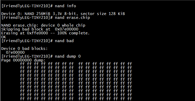
用友善的镜像做烧写文件系统的测试,用下面三条命令完成烧写yaffs2文件系统(注:在烧写yaffs2时要擦除0xe00000开始后面所有的块中的数据,否则会由于残存的数据影响Android启动)
烧写过程如下图:

启动信息如下图:(注:若在校正触摸屏出现Calibration failed.的问题,多尝试校正(保存)几次就通过了。测试时偶尔出现过这个问题。)
